
 By Nana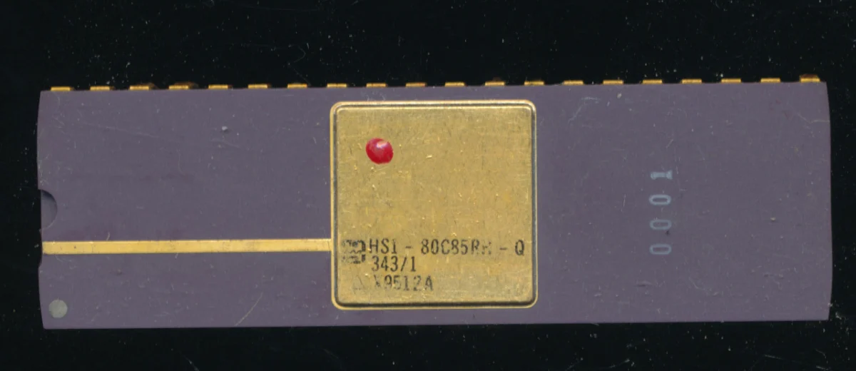
In the high-stakes world of aerospace and nuclear defense, the difference between mission success and catastrophic failure is often measured in microscopic tolerances. During the late 1970s and early 1980s, as the Cold War reached its technological zenith, Sandia National Laboratories in Albuquerque, New Mexico, embarked on a mission that would redefine the limits of electronic resilience. To ensure the reliability of strategic weapons and deep-space probes, Sandia developed an internal capacity to design, fabricate, and test integrated circuits (ICs) that could withstand environments lethal to both humans and standard commercial hardware.
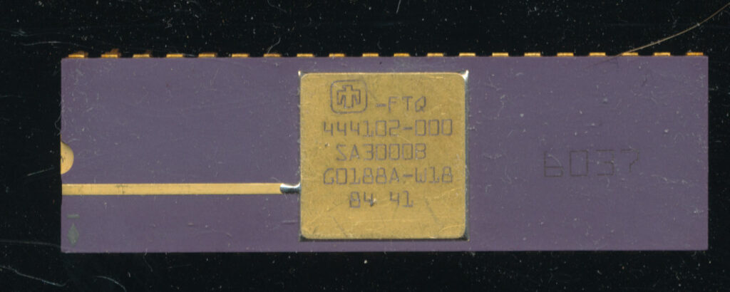
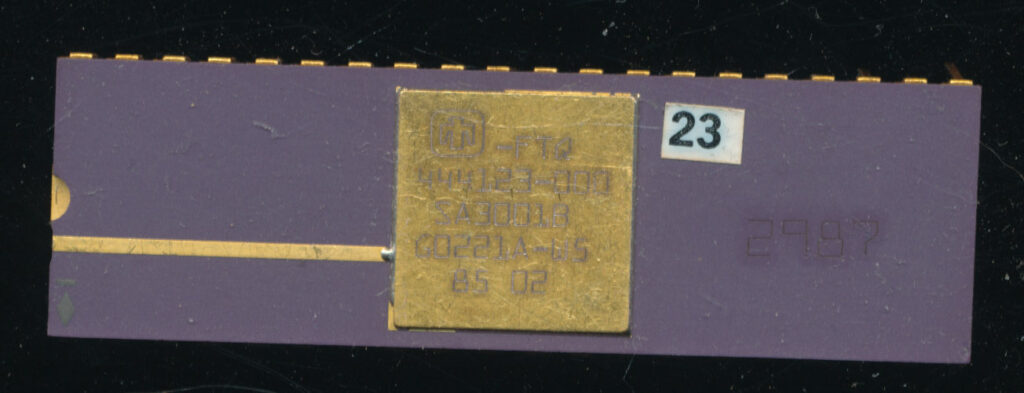
At the heart of this endeavor was the SA3000, a radiation-hardened iteration of the ubiquitous Intel 8085 processor. This device did more than just compute; it became the silent guardian of some of the most sensitive systems ever built by the United States government.
The Mandate for Resilience: Why a National Lab Needed a Fab
In the late 1970s, the commercial semiconductor market was prioritizing speed, cost, and miniaturization. However, the Department of Energy and the Department of Defense required something fundamentally different: “rad-hard” (radiation-hardened) electronics. Standard chips were prone to "latchup"—a condition where radiation causes a short circuit that can destroy a device—or "bit flips," which could cause critical calculation errors in a guidance system or a spacecraft.

When commercial vendors could not provide components capable of operating in the high-radiation environments of space or the interior of a nuclear warhead, Sandia took matters into its own hands. Beginning in 1978, the laboratory established a specialized fabrication facility. Initially working on 2-inch wafers with a 10-micron process, Sandia operated several generations behind the state-of-the-art commercial fabs of the day. By 1982, the facility had upgraded to 4-inch wafer capabilities with 2-micron feature sizes, allowing for the density required for complex processing tasks.
Chronology: From Concept to Deployment
The development of the SA3000 and its supporting ecosystem did not occur in a vacuum; it was part of a broader trajectory of mission-critical hardware development.
- 1978: Sandia launches its internal semiconductor fabrication facility, focusing on rad-hard process development.
- 1982: The lab achieves a 4-inch wafer production capability with 2-micron feature sizing. This infrastructure becomes the backbone for the Galileo space probe’s logic requirements.
- 1982–1984: Sandia engineers undertake the arduous task of converting the NMOS-based Intel 8085 to a CMOS-based rad-hard architecture.
- 1984: The SA3000 enters production. The design is optimized for high-voltage operation to combat the performance degradation caused by ionizing radiation.
- 1984–1985: A controversial federal mandate brings in Allied Signal to manage the fab, a decision that reportedly created significant friction and initial production bottlenecks.
- 1990: Harris Corporation commercializes the technology, releasing the HS1-80C85RH (space grade) and HS9-80C85RH (military grade).
- Present Day: The SA3000 remains a cornerstone of the W88 nuclear warhead’s guidance and fuzing systems, proving the longevity of robust, "old-school" engineering.
Engineering the Impossible: The SA3000 Architecture
The transition from the commercial Intel 8085—which utilized roughly 6,500 transistors—to the Sandia SA3000 was a massive undertaking. The final CMOS-based SA3000 contained approximately 18,000 transistors. The most significant design challenge was the instruction decoder, typically implemented as a Programmable Logic Array (PLA). While PLAs are efficient in NMOS logic, their translation to CMOS required creative engineering to maintain the necessary radiation immunity.

Hardening Techniques
Designing for radiation hardness is as much an art as it is a science. The Sandia team employed several critical techniques:
- Epitaxial Substrates: The chips were built on an n-on-n+ epitaxial substrate, which significantly reduced the risk of parasitic latchup.
- Guard Rings: Extensive guard rings were placed around individual transistors to isolate them from substrate interference.
- Hardened Oxides: By strictly controlling production temperatures, engineers created oxides that were far less susceptible to the charge buildup caused by ionizing radiation.
- Voltage Headroom: While commercial chips were limited to 5V, the SA3000 was designed to operate between 4.5V and 11V. This higher voltage range provided a critical buffer, as radiation exposure inherently slows the speed of a device. By running at higher voltages, the chip maintained its operational integrity even as the silicon degraded under intense radiation.
Supporting the Mission: Galileo and Beyond
The necessity for such specialized hardware was underscored by the Galileo mission to Jupiter. Sandia engineers were tasked with recreating the RCA 1802 processor and its associated support chips, ensuring they could survive the harsh radiation belts surrounding Jupiter. Over 50,000 individual ICs were produced for the probe, including backup sets and extensive testing hardware.
Beyond space exploration, the SA3000 became the "brain" for the W88 475kt nuclear warhead. It manages the critical fuzing and altitude calculations required for high-precision deployment. This application alone necessitated a "war reserve" stock, ensuring that even decades later, replacement parts remain available for the nation’s strategic deterrent.
Commercialization and External Oversight
The 1984 decision to introduce Allied Signal as a contractor to manage the Sandia fab was met with internal resistance. Critics argued that the move sacrificed the laboratory’s agility and deep institutional knowledge in favor of bureaucratic oversight. Despite these administrative hurdles, the technology was eventually matured enough to be licensed.
In 1990, Harris Corporation brought these designs to the wider aerospace and defense market. The resulting HS1-80C85RH and HS9-80C85RH chips offered a more accessible version of the Sandia tech. While they were limited to a 5V operating voltage and a 2MHz clock speed—compared to the 10MHz peak capability of the internal SA3000—they provided a critical supply chain for military and space contractors who required radiation tolerance without the need for custom, in-house fabrication.
Implications for Modern Computing
The performance metrics of the SA3000 were nothing short of extraordinary for the era. The chip was designed to withstand 1×10⁵ rads of radiation; however, in testing, it performed with only a 25% drop in performance at 1×10⁶ rads, and remained functional even at 3×10⁶ rads. To put this in perspective, a dose of 1,000 rads is typically fatal to a human, illustrating the extreme disparity between biological and silicon-based resilience in high-energy environments.
The legacy of the SA3000 serves as a reminder of the trade-offs in engineering. While the modern world chases the next nanometer of shrinkage, the defense and aerospace sectors often find their most reliable solutions in older, hardened, and battle-tested architectures.
The longevity of the SA3000 in the W88 warhead demonstrates a fundamental principle of engineering: when the environment is extreme and the stakes are existential, the complexity of the design must be balanced by the simplicity and robustness of its execution. Sandia National Laboratories didn’t just build a processor; they built a standard for reliability that has, in some cases, endured for over forty years, effectively defying the rapid obsolescence of the semiconductor industry.
As we look toward future space exploration, from missions to the icy moons of Jupiter to deep-space autonomous probes, the lessons learned from the SA3000—the importance of substrate isolation, the value of high-voltage headroom, and the necessity of radiation-hardened oxides—remain the bedrock of modern aerospace electronic design.
 rifanmuazin
  Layla Zulfa
  Evan Lee Salim