
 By Neng Nana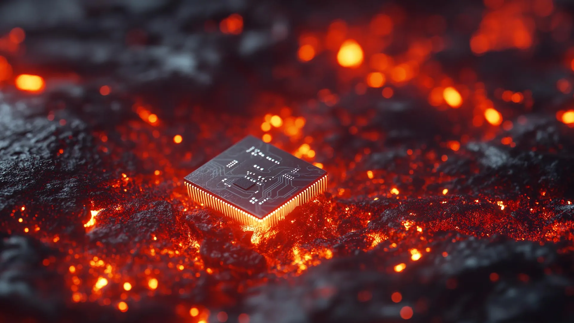
For decades, the field of modern electronics has operated under an invisible but absolute ceiling. From the smartphone in your pocket to the complex sensors aboard interplanetary satellites, silicon-based technology has been constrained by a fundamental vulnerability: heat. Once temperatures climb past the 200-degree Celsius mark, the delicate architecture of standard electronics begins to degrade, leading to system failure, data corruption, and catastrophic hardware meltdown. This thermal barrier has long dictated the limits of space exploration, deep-earth drilling, and high-performance industrial machinery.
However, a groundbreaking study published on March 26, 2026, in the journal Science suggests that this decades-old limitation is finally being dismantled. A research team led by Joshua Yang, the Arthur B. Freeman Chair Professor at the USC Viterbi School of Engineering and the USC School of Advanced Computing, has unveiled a revolutionary memory device capable of operating at 700 degrees Celsius (~1300 degrees Fahrenheit)—a temperature higher than molten lava. This achievement does not merely push the boundaries of current technology; it renders the previous state-of-the-art obsolete.
The Architecture of Resilience: The High-Temperature Memristor
At the heart of this discovery is a nanoscale component known as a "memristor." Unlike traditional binary memory, which functions strictly as a storage medium, a memristor is a sophisticated component that can store data and perform complex computations simultaneously.
The device, developed by lead author Jian Zhao and his colleagues, is engineered as a microscopic layered structure. Its composition is the secret to its thermal invincibility. The team utilized tungsten for the top electrode—a metal renowned for having the highest melting point of any element—and a middle layer of hafnium oxide, a robust ceramic material. The breakthrough, however, lies at the bottom layer: a single-atom-thick sheet of graphene.
Graphene, a hexagonal lattice of carbon atoms, is famed for its exceptional strength and heat resistance. By pairing this material with tungsten, the researchers created an interface that behaves in an unexpected, highly beneficial way. In conventional electronic designs, heat induces "atomic migration," where metal atoms from the electrode slowly drift through the ceramic layer. Over time, these atoms form a conductive filament, creating a permanent short circuit that leaves the device stuck in an "on" state.
The graphene layer acts as an impenetrable barrier to this migration. As Professor Yang described it, the interaction between the tungsten and the graphene is akin to "oil and water." Because the tungsten atoms cannot find a stable surface to bond with on the graphene, they drift away rather than forming the short-circuiting bridge that typically destroys electronic components.
A Chronology of Discovery: From Failure to Innovation
The path to this discovery was far from a linear progression. In fact, the team was not initially searching for a heat-resistant memory chip at all. The project began as an attempt to develop a different, graphene-based electronic device, but the experimental prototype failed to perform as the team had intended.
"To be honest, it was by accident, as most discoveries are," Yang noted. "If you can predict it, it’s usually not surprising, and probably not significant enough."
Rather than abandoning the failed prototype, the team analyzed the device’s unexpected behavior under thermal stress. Through a combination of advanced electron microscopy, spectroscopy, and high-level quantum simulations, they discovered the "oil and water" repulsion mechanism that prevented the device from failing. Once they identified the principle behind this unexpected durability, the team refined the structure to test its limits.
In subsequent trials, the device proved to be remarkably stable. It retained data for over 50 hours at 700 degrees Celsius without requiring a refresh, and it endured more than one billion switching cycles—the process of writing and erasing data—at that same extreme temperature. Operating at a mere 1.5 volts with switching speeds in the tens of nanoseconds, the device demonstrated that high-temperature resilience does not necessarily come at the cost of power efficiency or speed.
Supporting Data and Technical Validation
The technical specifications of the new memristor place it in a league of its own. While standard commercial electronics are generally rated for operation up to 125 degrees Celsius—the heat levels often encountered in automotive engine environments—the USC team’s device showed no signs of degradation at 700 degrees.
Crucially, the researchers noted that 700 degrees was simply the limit of their laboratory testing equipment, suggesting that the device’s true operating threshold may be significantly higher. The use of mature materials like tungsten and hafnium oxide—both of which are already cornerstones of the semiconductor manufacturing industry—provides a clear, albeit challenging, path toward industrial-scale production. While graphene is a more exotic material, it is already being integrated into manufacturing workflows by tech giants like TSMC and Samsung, indicating that the supply chain for this high-temperature technology is already beginning to mature.
Implications for Industry and Exploration
The implications of a computer chip that can function in the heart of a furnace are profound. The most immediate application lies in the field of space exploration. Current landers sent to planets like Venus—where surface temperatures hover around 460 degrees Celsius—must be equipped with massive, heavy cooling systems and reinforced pressurized housings to protect their delicate electronics. A chip that can survive these environments natively would drastically reduce the size, weight, and cost of space missions, allowing for longer-duration, more capable probes.
Beyond the atmosphere, the technology has vast potential in terrestrial industries:
- Geothermal Energy: Deep-earth exploration requires sensors capable of operating in high-temperature, high-pressure environments where current silicon-based electronics fail almost instantly.
- Nuclear and Fusion Systems: The ability to place control logic and sensors in direct proximity to radioactive, high-heat environments would revolutionize the monitoring and safety protocols of next-generation nuclear reactors.
- Automotive and Aerospace: Even in less extreme conditions, the inherent durability of this design offers a "buffer" that would significantly extend the lifespan of electronics in harsh operating environments, reducing the risk of failures that cause safety recalls and maintenance headaches.
A New Frontier for Artificial Intelligence
Perhaps the most exciting, if unexpected, application of the high-temperature memristor is in the realm of Artificial Intelligence (AI). As global demand for AI increases, the limitations of traditional computing have become a bottleneck. Modern AI systems rely almost exclusively on "matrix multiplication"—a mathematical process that requires moving vast amounts of data between memory and a processor. This "von Neumann bottleneck" is energy-intensive and creates significant heat, which in turn limits how powerful AI chips can be.
The memristor solves this by performing the computation directly within the memory component. By utilizing Ohm’s Law, the device computes the result of a multiplication as electricity flows through the material, effectively turning the memory chip into an analog processor.
"Over 92 percent of the computing in AI systems like ChatGPT is nothing but matrix multiplication," Yang explained. "This type of device can perform that in the most efficient way, orders of magnitude faster and at lower energy."
Professor Yang and his collaborators—Qiangfei Xia, Miao Hu, and Ning Ge—have already co-founded a company called TetraMem to bring memristor-based AI chips to the commercial market. While their current work with TetraMem is focused on room-temperature AI, the new 700-degree breakthrough provides a roadmap for "extreme AI"—computing that can take place in the field, on a factory floor, or in deep space, without the need for centralized data centers.
Official Responses and Future Outlook
The research was conducted under the auspices of the CONCRETE Center (Center of Neuromorphic Computing under Extreme Environments), a multi-university collaboration led by USC and backed by the Air Force Office of Scientific Research and the Air Force Research Laboratory. This partnership highlights the strategic importance of the discovery for national defense and aerospace technology.
Despite the excitement, the team remains grounded in the realities of engineering. "This is the first step," Yang said. "It’s still a long way to go."
While the memory component itself is now viable, a complete computer requires logic gates, sensors, and power management systems that can also withstand these temperatures. Furthermore, moving from a manually constructed lab prototype to a mass-produced industrial product is a multi-year endeavor. Nevertheless, the researchers believe that by establishing the fundamental principles of high-temperature resilience at the atomic level, they have provided the "missing piece" of the puzzle.
As the team looks toward the future, the sentiment is one of optimism. For Yang, the publication in Science is not just a victory for materials science, but a signal of a new era. "Space exploration has never been so real, so close, and at such a large scale," he said. "This paper represents a critical leap into a much larger, more exciting frontier." By breaking the thermal barrier, the researchers at USC have not only created a more durable chip; they have opened the door to a world where our machines can go where humans have never dared to send them, and perform tasks that were previously deemed impossible.
 Sagoh
Sagoh  Asro
Asro  Siti Muinah