
 By Basiran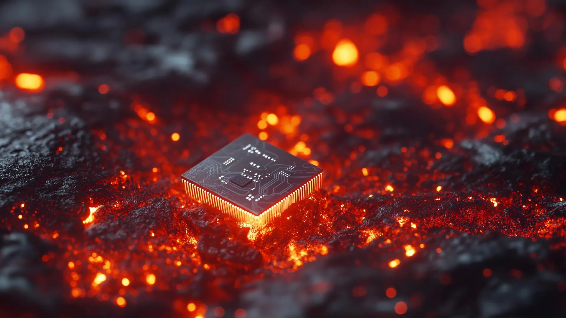
For decades, the march of technological progress has been dictated by a rigid, invisible boundary: the thermal limit. From the microprocessors in our smartphones to the complex avionics guiding deep-space probes, modern electronics are tethered to a fragile reality. Once ambient or operational temperatures climb above 200 degrees Celsius, the delicate architecture of silicon-based chips begins to falter, leading to catastrophic failure. This "thermal wall" has long been the primary adversary of engineers seeking to push technology into the most extreme corners of our universe—and even into the high-heat environments of our own planet’s crust.
Now, a team of researchers at the University of Southern California (USC) has announced a breakthrough that may effectively demolish this ceiling. In a study published on March 26, 2026, in the journal Science, a team led by Joshua Yang, the Arthur B. Freeman Chair Professor at the Ming Hsieh Department of Electrical and Computer Engineering, unveiled a new class of memory device capable of operating flawlessly at 700 degrees Celsius (approximately 1,300 degrees Fahrenheit).
This temperature, which exceeds the heat of molten lava, represents a quantum leap in material science. The device did not merely survive these conditions; it exhibited no signs of degradation, limited only by the maximum thermal threshold of the researchers’ own testing equipment.
The Chronology of a Serendipitous Discovery
The path to this discovery was not paved with a linear, predetermined roadmap. In the high-stakes world of semiconductor research, breakthroughs often arrive not through expected milestones, but through the patient observation of anomalies.
The research team, which included first author Jian Zhao and collaborators from the Air Force Research Laboratory (AFRL) and Kumamoto University, was originally working on an entirely different objective: developing a graphene-based component for standard electronic applications. During the prototyping phase, the device failed to perform as predicted in their initial experiments. However, rather than discarding the results as a failed trial, the team scrutinized the unexpected behavior.
"To be honest, it was by accident, as most discoveries are," said Professor Yang. "If you can predict it, it’s usually not surprising, and probably not significant enough."
Following the initial observation, the team pivoted to analyze why the device exhibited such anomalous resilience to heat. By employing a combination of advanced electron microscopy, high-resolution spectroscopy, and quantum-level simulations, the researchers identified the physical mechanism preventing the "short-circuiting" that plagues traditional electronics. This iterative process—from a failed experiment to a deep-dive forensic analysis of atomic behavior—transformed a lab-bench error into a revolutionary design principle.
Engineering the Unstoppable: The Memristor Architecture
At the heart of this innovation is the "memristor"—a nanoscale electronic component that functions as both a data storage unit and a computational engine. Unlike a standard transistor, which relies on binary logic gates, the memristor possesses a "memory" of the amount of charge that has previously flowed through it, allowing it to modulate its resistance.
To achieve the 700-degree threshold, the USC team engineered a precise, layered structure:
- The Top Electrode: Constructed from tungsten, an element holding the distinction of having the highest melting point of any metal in the periodic table.
- The Core: A thin layer of hafnium oxide ceramic, which provides the necessary insulating properties and stability.
- The Bottom Layer: A single-atom-thick sheet of graphene.
The interaction between these materials is the key to the device’s durability. In conventional electronics, heat acts as a catalyst for "metal migration." Under high thermal stress, metal atoms from the electrode tend to drift through the insulating ceramic, eventually creating a conductive filament that causes a short circuit.
The USC team discovered that the graphene layer acts as an impenetrable barrier to this migration. Using an analogy provided by Yang, the relationship between the tungsten and the graphene is akin to "oil and water." Tungsten atoms, when approaching the graphene surface, find no stable site to latch onto. Instead of forming a conductive bridge through the ceramic, they simply drift away. This elegant physical exclusion keeps the device’s integrity intact, even under conditions that would liquify or vaporize conventional components.
Supporting Data and Performance Metrics
The data generated during the testing phase was nothing short of extraordinary. The device was subjected to a sustained 700-degree environment for over 50 hours, during which it retained stored data without the need for periodic refreshing—a common requirement in many memory types.
Furthermore, the component demonstrated remarkable operational stamina:
- Switching Cycles: The device endured more than one billion switching cycles while maintained at 700 degrees Celsius, showing no measurable wear.
- Voltage Efficiency: It operated at a remarkably low power draw of just 1.5 volts.
- Response Time: Switching speeds were recorded in the range of tens of nanoseconds, proving that the device is not only durable but also fast enough for high-performance computing.
These metrics confirm that the device is not merely a theoretical curiosity; it is a functional, efficient, and robust piece of hardware that matches or exceeds the performance of traditional memory components while operating in a regime previously thought to be impossible.
Implications: From Venus to the Earth’s Core
The implications of a 700-degree-capable electronic component are vast, spanning both the macro-scale of industrial engineering and the astronomical scale of space exploration.
Space Exploration and the "Venus Problem"
For decades, the exploration of Venus has been hindered by the planet’s brutal surface conditions. With average temperatures hovering around 460 degrees Celsius and crushing atmospheric pressure, traditional silicon electronics fail within hours of landing. A memory device capable of surviving 700 degrees opens the door for long-duration, high-fidelity missions to Venus and even deeper into the interior of gas giants, where electronics could finally function in situ.
Industrial and Energy Applications
Beyond the atmosphere, the terrestrial applications are equally compelling.
- Geothermal Energy: Deep-earth drilling requires sensors and control systems that can withstand the intense heat of the Earth’s crust. Current systems require cumbersome cooling rigs; the USC-developed chips could allow for "down-hole" processing, providing real-time data from miles beneath the surface.
- Nuclear and Fusion Power: Environments within nuclear reactors and experimental fusion facilities are characterized by extreme heat and high radiation. High-temperature-resistant electronics could lead to more robust monitoring systems that enhance safety and operational efficiency.
- Automotive and Aerospace: While commercial engines operate below 700 degrees, the inherent durability of this technology suggests that automotive sensors—often subjected to the high heat of exhaust and engine blocks—could see their lifespans extended indefinitely, drastically reducing the risk of component failure.
A Paradigm Shift for Artificial Intelligence
Perhaps the most surprising application of this technology lies in the realm of Artificial Intelligence (AI). Modern AI systems, such as Large Language Models, rely almost exclusively on "matrix multiplication"—the repeated, intensive calculation of massive data sets. Traditional Von Neumann architecture, which separates the CPU from memory, creates a "bottleneck" where moving data back and forth consumes massive amounts of energy.
Memristors, however, perform these calculations directly in the memory, utilizing Ohm’s Law. Because the computation happens as electricity flows through the device, it is exponentially faster and more energy-efficient than traditional processing.
"Over 92 percent of the computing in AI systems like ChatGPT is nothing but matrix multiplication," Professor Yang noted. By integrating these heat-resistant memristors into AI hardware, we could see a future where AI processing is done at the "edge"—directly on sensors in extreme environments—rather than sending data back to a centralized server.
The Road to Commercialization
Despite the enthusiasm surrounding the discovery, the researchers remain pragmatic about the transition from lab prototype to consumer product.
"This is the first step," Yang said. "It’s still a long way to go."
While the memory device is a breakthrough, it is only one piece of the puzzle. To build a complete, high-temperature computer, the team must now develop logic circuits that can match the heat resistance of the memory. Additionally, the current manufacturing process is manual and small-scale. However, the path to industrial production is clearer than it might appear. Tungsten and hafnium oxide are already staples in the semiconductor industry, and graphene—once considered a lab-only material—is now being integrated into wafer-scale production by industry giants like TSMC and Samsung.
The research, conducted under the umbrella of the CONCRETE Center (Center of Neuromorphic Computing under Extreme Environments) and supported by the Air Force Office of Scientific Research, is a testament to the power of collaborative, interdisciplinary science.
As the team looks to the future, the goal is clear: to continue refining the technology and, eventually, to see it deployed in the field. For Professor Yang, the publication in Science is more than just a successful experiment—it is an invitation to explore a new frontier. "Space exploration has never been so real, so close, and at such a large scale," he said. "This paper represents a critical leap into a much larger, more exciting frontier."
 Sagoh
Sagoh  Asro
Asro  Siti Muinah