
 By rifanmuazin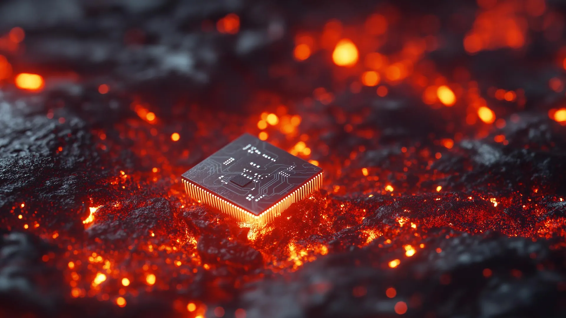
For over half a century, the progress of modern electronics has been defined by a relentless drive toward miniaturization and speed. From the microchips powering our smartphones to the sophisticated avionics guiding deep-space probes, our technological civilization rests on a foundation of silicon. Yet, this foundation has a brittle Achilles’ heel: heat.
In standard electronics, once temperatures climb above 200 degrees Celsius, the laws of thermodynamics begin to dismantle the device. Atomic migration causes short circuits, semi-conductive properties degrade, and the delicate architecture of a processor collapses. This "thermal barrier" has long served as an invisible ceiling for aerospace engineering, geothermal exploration, and industrial automation.
However, a groundbreaking study published on March 26, 2026, in the journal Science suggests that this ceiling has finally been shattered. A team of researchers led by Joshua Yang at the University of Southern California (USC) has unveiled a new type of memory device capable of operating at 700 degrees Celsius—a temperature that exceeds that of molten lava.
The Anatomy of an Unexpected Discovery
The breakthrough centers on a device known as a memristor—a nanoscale component that acts as both a memory storage unit and a processing engine. Unlike traditional transistors, which require constant power to maintain data, memristors can "remember" their state, making them highly efficient for the next generation of artificial intelligence.
The device’s architecture is deceptively simple: a microscopic sandwich consisting of a tungsten top electrode, a hafnium oxide ceramic center, and a bottom layer of graphene. The choice of materials was deliberate, yet the realization of their potential was, as lead researcher Joshua Yang describes, a "happy accident."
The team was originally attempting to develop a different graphene-based component. When that project failed to yield the intended results, they noticed the device was exhibiting anomalous stability under extreme thermal stress. Upon closer inspection, they realized that the graphene layer was acting as an atomic barrier.
In conventional electronics, heat triggers the migration of metal atoms from the electrode into the ceramic insulation, creating a conductive bridge that permanently shorts out the chip. In the USC team’s device, the interaction between the tungsten and the graphene is akin to oil and water; the tungsten atoms are unable to anchor themselves to the graphene, preventing the formation of short circuits even at 700 degrees Celsius.
Chronology of the Breakthrough
The road to this discovery was paved with rigorous scientific investigation and, eventually, a moment of serendipity.
- Initial Research Phase: The team, operating under the umbrella of the CONCRETE Center (Center of Neuromorphic Computing under Extreme Environments), set out to engineer robust components capable of surviving harsh conditions.
- The Failure: Early in 2025, the researchers attempted to fabricate a specific graphene-based architecture. The experiment failed to meet the original design specifications.
- The Observation: During post-mortem testing of the failed components, researchers noted that the device did not degrade under high heat. Instead, it performed with unprecedented stability.
- Validation: Through the remainder of 2025, the team utilized advanced electron microscopy, spectroscopy, and quantum-level simulations to reverse-engineer why the device was succeeding where others failed.
- The Publication: On March 26, 2026, the findings were formally published in Science, detailing the mechanism behind the thermal resilience and confirming the device’s operational capacity at 700°C.
Supporting Data: Testing the Limits
The performance metrics of the new memristor are striking. During testing, the device demonstrated:
- Data Retention: It held stored data for over 50 hours at a constant 700°C without the need for an energy-draining "refresh" cycle.
- Endurance: The component successfully completed over one billion switching cycles at the same temperature, showing no signs of fatigue.
- Operational Efficiency: The device operates at a low voltage of 1.5 volts with switching speeds in the tens of nanoseconds.
Crucially, 700 degrees Celsius was not the point of failure for the device; it was merely the maximum limit of the testing equipment available to the researchers. The team suspects that the device could potentially withstand even higher temperatures, though further verification is required.
Official Perspectives and Expert Insight
Joshua Yang, the Arthur B. Freeman Chair Professor at the Ming Hsieh Department of Electrical and Computer Engineering at USC, frames this as a paradigm shift. "You may call it a revolution," Yang noted in a recent briefing. "It is the best high-temperature memory ever demonstrated. If you can predict a discovery, it’s usually not surprising, and probably not significant enough. This was an accident, but it has turned into a principle that will guide future designs."
The research is a flagship project of the CONCRETE Center, a multi-university collaboration supported by the Air Force Office of Scientific Research and the Air Force Research Laboratory (AFRL). Dr. Sabyasachi Ganguli and his team at the AFRL Materials Lab in Dayton, Ohio, provided critical experimental support, while theoretical insights were bolstered by collaborators at Kumamoto University in Japan.
"Space exploration has never been so real, so close, and at such a large scale," Yang said. "This paper represents a critical leap into a much larger, more exciting frontier."
Implications: A New Era for AI and Exploration
The implications of this technology are vast, spanning from the surface of Venus to the depths of the Earth’s crust.
Space Exploration and Harsh Environments
Current robotic landers sent to planets like Venus—where surface temperatures hover around 500 degrees Celsius—suffer from rapid hardware failure. Engineers are forced to build heavy, bulky cooling systems or radiation-hardened shielding that drastically reduces the scientific payload. A computer that can operate at 700 degrees without cooling systems could enable lighter, more capable landers, effectively opening the door to long-term exploration of Venusian, Jovian, and solar-proximate environments.
Industrial and Geothermal Utility
Deep-earth drilling for geothermal energy often involves environments where surrounding rock glows red-hot. Currently, sensors must be retracted frequently to prevent destruction. High-temperature memristors would allow for "down-hole" computing, enabling real-time data processing in environments previously considered hostile to electronics. Similar benefits apply to nuclear and fusion energy systems, where intense heat currently limits the placement of control sensors.
The Future of Artificial Intelligence
Perhaps the most immediate commercial application lies in the efficiency of AI. Modern AI relies on matrix multiplication—the fundamental mathematical operation behind image recognition and language models. Traditional computers move data between memory and processors, which is energy-intensive.
Memristors perform these calculations directly as current flows through the component, using Ohm’s Law to derive the result instantly. "Over 92 percent of the computing in AI systems like ChatGPT is nothing but matrix multiplication," Yang explains. "This type of device can perform that in the most efficient way, orders of magnitude faster and at lower energy."
Moving Toward Commercialization
Despite the excitement, the team remains grounded. Yang and his co-founders—Qiangfei Xia, Miao Hu, and Ning Ge—have already established a company, TetraMem, to focus on room-temperature memristor chips. While TetraMem is already using these chips for machine learning tasks, the high-temperature variant is currently in the prototype stage.
Translating a lab-grown component into a mass-manufactured product involves several hurdles:
- Integration: Memory is only one component. The team must now develop high-temperature logic circuits to work alongside these memory cells.
- Scalability: The current devices were hand-fabricated. Transitioning to large-scale semiconductor wafer manufacturing will require significant engineering.
- Material Supply Chain: Tungsten and hafnium oxide are already staples of the semiconductor industry. Graphene, while more challenging, is currently being scaled by giants like TSMC and Samsung, suggesting that the supply chain infrastructure is maturing alongside the technology.
"This is the first step," Yang concluded. "It’s still a long way to go, but logically, you can see: now it makes it possible. The missing component has been made."
As the scientific community digests these findings, the path forward appears clear. By mastering the interface between atomic structures and extreme thermal environments, the USC team has not only solved a decades-old engineering bottleneck but has also provided a blueprint for the next generation of computing—a generation that will thrive where silicon once feared to tread.
 Sagoh
Sagoh  Asro
Asro  Siti Muinah