
 By Evan Lee Salim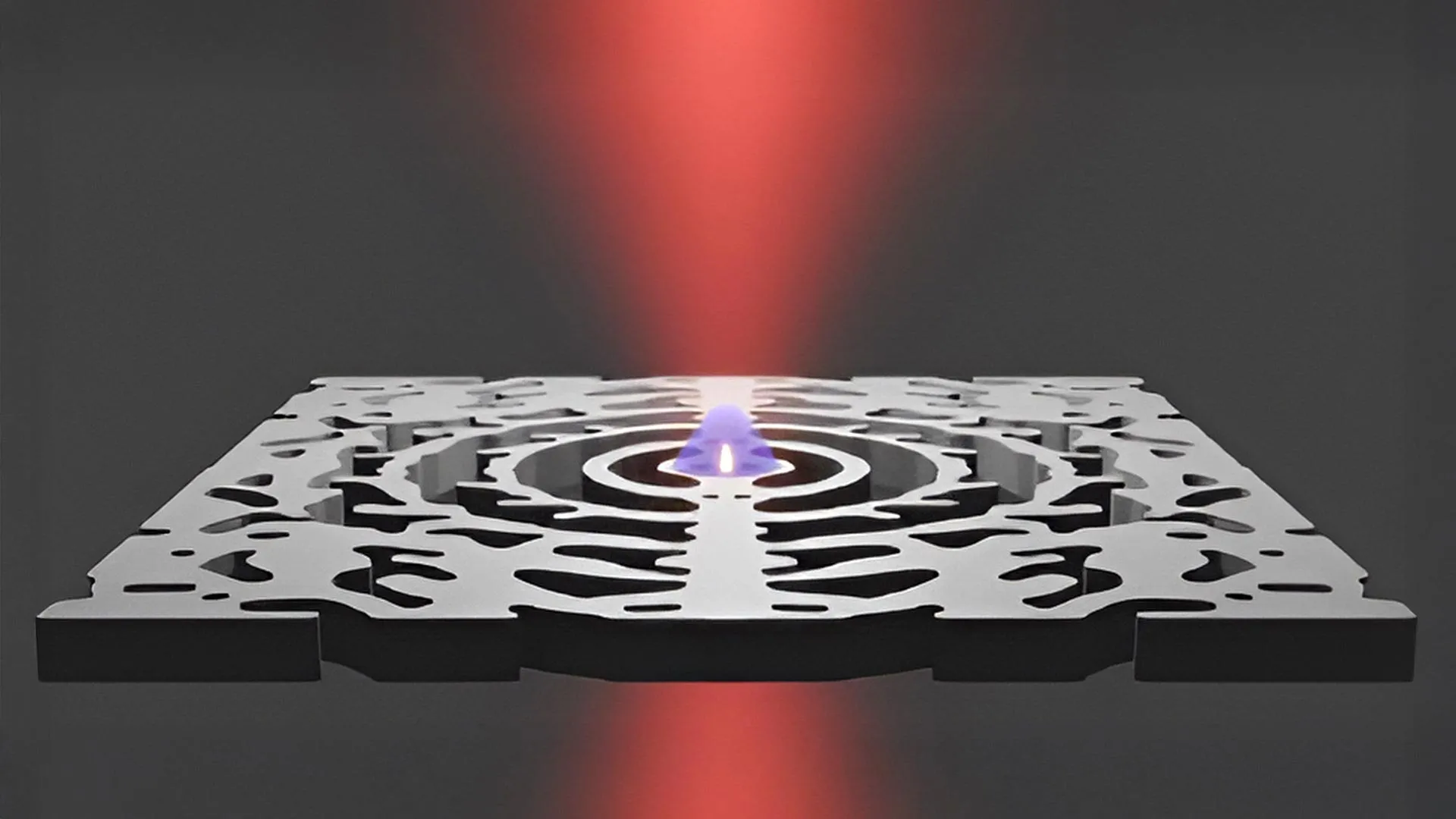
The landscape of modern computing stands at a critical juncture. For decades, the relentless march of Moore’s Law has driven the miniaturization of transistors, packing ever-increasing amounts of processing power into the palm of our hands. Yet, we are hitting a physical wall: heat. As electronic circuits shrink, the movement of electrons through copper pathways generates significant thermal energy, creating a bottleneck that limits speed and consumes vast amounts of electricity.
Now, a team of researchers at the Technical University of Denmark (DTU) has unveiled a breakthrough that may fundamentally alter this trajectory. By developing a revolutionary nanolaser capable of being integrated directly onto microchips, these scientists have opened the door to a future where data is transmitted not by the sluggish, heat-generating flow of electrons, but by the near-instantaneous, energy-efficient pulse of light.
The Core Innovation: Moving Beyond Electrons
For the global internet, light is already the gold standard. Fiber optic cables carry the world’s data across oceans and continents using pulses of light, which travel with minimal loss and immense bandwidth. However, once that signal reaches a computer, smartphone, or server, it must be converted back into electrical signals to be processed. This conversion process is slow, energy-intensive, and generates the very heat that plagues modern high-performance computing.
The nanolaser developed by the DTU team, led by Professor Jesper Mørk alongside Drs. Meng Xiong and Yi Yu, represents a bridge between the photonic world of telecommunications and the electronic world of silicon chips. By generating light signals directly on the chip, researchers can bypass the need for power-hungry electrical data transmission, potentially ushering in an era of "optical computing."
Chronology: From Concept to Clean Room
The development of this technology did not happen in a vacuum; it is the culmination of years of interdisciplinary collaboration at DTU.
- The Foundational Phase: The project began with a fundamental question: How can we confine light into a space smaller than its own wavelength without losing its energy? The answer came from the synergy between DTU Electro and DTU Construct. The light-trapping structure at the heart of the nanolaser was originally developed by Professor Ole Sigmund’s group at DTU Construct, using sophisticated mathematical modeling to design structures that defy traditional optical limits.
- The Fabrication Phase: With a design in hand, the team moved to DTU Nanolab, the university’s state-of-the-art clean room facility. Here, the researchers faced the monumental task of manufacturing a device that pushed the theoretical limits of laser physics.
- The Validation Phase: Following fabrication, the team subjected the nanolaser to rigorous testing. They observed that when a beam of light was shone onto the device, photons and electrons were concentrated in a microscopic region—a nanocavity—allowing the laser to function at room temperature.
- The Publication: The results were published in the peer-reviewed journal Science Advances, marking a formal entry of this technology into the global scientific discourse.
Supporting Data: Why Size Matters
To understand the significance of the DTU nanolaser, one must look at the physics of light confinement. Conventional lasers are relatively large, often requiring bulky mirrors and power sources. A nanolaser, by contrast, operates on the scale of a few hundred nanometers—roughly the size of a virus.
Professor Jesper Mørk emphasizes that the DTU device pushes beyond the conventional "diffraction limit," a rule that has historically dictated how small a laser can be. By utilizing a nanocavity to trap light in an exceptionally tiny space, the researchers have achieved a level of light intensity previously thought to be impossible at this scale.
The potential efficiency gains are staggering. Mørk estimates that by replacing traditional electronic interconnects with these optical pathways, future computer systems could reduce their total energy consumption by as much as 50%. In the world of data centers—which currently account for a significant and growing percentage of global electricity usage—a 50% reduction would be a transformative contribution to climate goals.
Official Responses and Expert Insights
The research team, which includes Drs. Meng Xiong and Yi Yu, underscores that this is not merely a laboratory curiosity but a roadmap for industrial application.
"The nanolaser opens up the possibility of creating a new generation of components that combine high performance with minimal size," says Professor Jesper Mørk. He highlights that the application is twofold:
- IT Infrastructure: Reducing the energy cost of moving data, which is the primary driver of power usage in modern supercomputers.
- Healthcare Innovation: Because the nanolaser can concentrate light with such extreme precision, it creates a powerful tool for ultra-sensitive biosensors and high-resolution imaging, allowing for medical diagnostics that were previously impossible at the bedside.
The Roadmap Ahead: Technical Challenges and Future Implications
Despite the excitement surrounding the publication, the team is pragmatic about the road ahead. The current prototype is optically pumped, meaning it requires an external light source to trigger its operation. The next, and perhaps most difficult, hurdle is achieving "electrically pumped" operation.
The Path to Electrically Powered Nanolasers
If the researchers can successfully transition the laser to run on standard electrical current—the same power that runs a modern CPU—the integration into commercial smartphones and laptops becomes a reality.
- The 5–10 Year Horizon: The DTU team estimates that the remaining technical challenges can be solved within the next five to ten years. This timeline aligns with the expected industry shifts toward more specialized, energy-efficient silicon architectures.
- Climate and Economic Impact: Beyond the speed of a faster smartphone, the broader economic impact lies in the sustainability of the global digital infrastructure. As the world moves toward an AI-driven economy, the demand for data processing is skyrocketing. If the hardware running these processes cannot become more efficient, the energy costs will become unsustainable. Nanolasers represent one of the few viable paths to scaling processing power without scaling carbon footprints.
Implications for Healthcare and Sensing
The implications extend far beyond the motherboard. In the field of medicine, the ability to integrate nanolasers into "lab-on-a-chip" devices could revolutionize diagnostics. By using these lasers to probe biological samples at the molecular level, healthcare providers could identify diseases at their earliest stages, moving from reactive medicine to proactive, precision health management.
Conclusion: A Paradigm Shift in Computing
The transition from electronic-based computing to photonic-based communication is often compared to the transition from copper wire telegraphs to fiber optic networks. It is a fundamental shift in the medium of information. While we are still in the early stages of this transition, the work being done at DTU provides the essential hardware foundation required to make it happen.
As thousands of these tiny, efficient lasers find their way onto a single microchip, the limitations of today’s devices—heat, energy waste, and speed bottlenecks—will begin to fade. We are looking at a future where our devices are cooler, faster, and significantly more efficient. The DTU nanolaser is more than just a small component; it is a glimpse into the future of a world powered by light.
As Professor Mørk and his colleagues look toward the next decade of development, the scientific community watches with anticipation. If they succeed, the history of computing will be divided into two distinct eras: the era of the electron, and the era of the photon. And the transition, quite literally, will be illuminated by the nanolaser.
 Asro
Asro  Sagoh
Sagoh  Dwi Wanna