
 By Lina Hope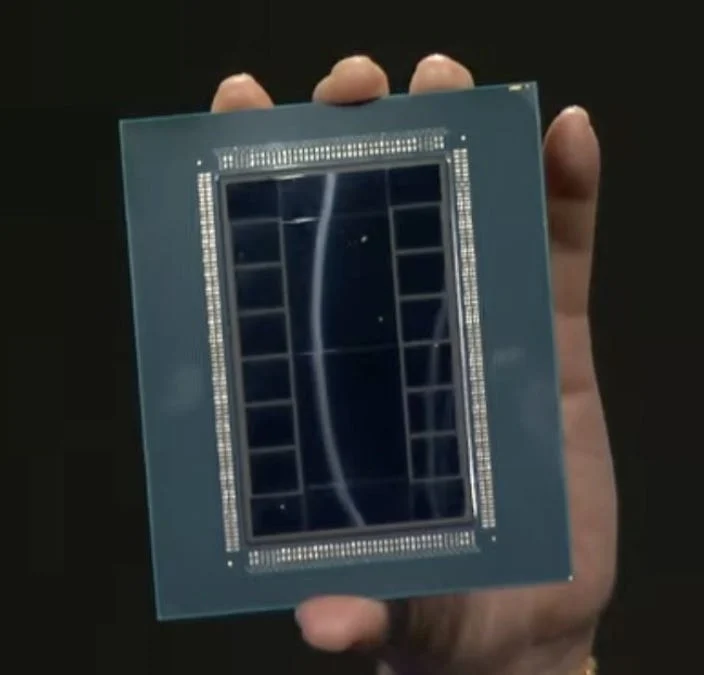
As the semiconductor industry braces for AMD’s highly anticipated "Advancing AI" event, the technical community has turned its attention to the low-level architecture of the company’s next-generation hardware. By meticulously analyzing recent LLVM (Low-Level Virtual Machine) compiler commits, we can begin to assemble a high-fidelity picture of the upcoming MI400 series. These accelerators, specifically the GFX1250, represent a pivotal shift in AMD’s silicon strategy, blending the agility of consumer RDNA architectures with the raw, high-performance compute capabilities required for the next era of AI infrastructure.
Main Facts: The Emergence of GFX1250 and GFX1251
The LLVM codebase has provided early, preliminary support for two distinct accelerators: the GFX1250 and the GFX1251. These are not merely iterative upgrades; they are targeted tools designed for the diverging needs of the modern data center.
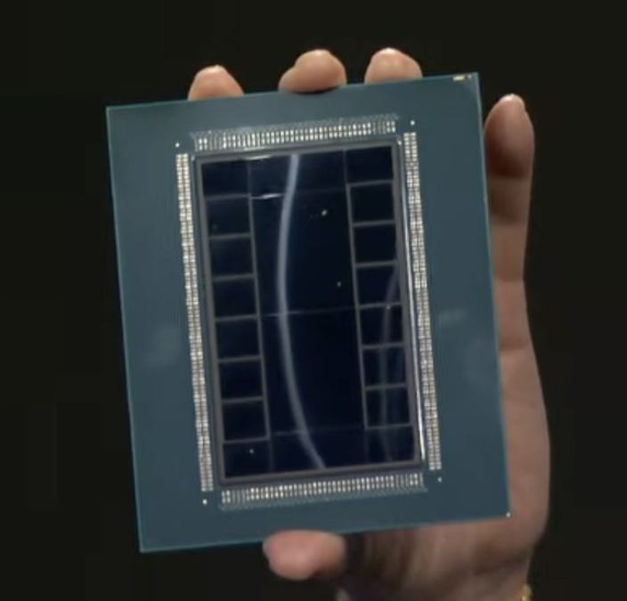
The GFX1250, marketed as the MI455X, is the primary engine for AMD’s forthcoming Helios rack platform, a system specifically engineered to dominate the machine learning market. In parallel, the GFX1251 targets the High-Performance Computing (HPC) sector. Labeled as the MI430X, this variant is projected by AMD to deliver a staggering 200 TFLOPs of native double-precision (FP64) compute, positioning it as a heavyweight contender against the industry’s most powerful HPC offerings.
While the GFX1251 warrants a deep dive of its own, the current architectural focus lies firmly on the MI455X (GFX1250). It appears to be a "pure" compute accelerator, with many traditional graphics features stripped away to optimize for die space and performance density.
Architectural Evolution: A Convergence of Philosophies
The GFX1250 architecture presents a fascinating study in convergence. Historically, AMD’s consumer (RDNA) and data center (CDNA) lines maintained distinct design philosophies. The GFX1250, however, seems to act as a bridge.
The WGP and Cache Hierarchy
A curious observation in the LLVM documentation is the classification of these accelerators as "APUs," though they clearly function as discrete datacenter GPUs. Furthermore, the "Workgroup Processor" (WGP) design has been refined. While previous generations treated the WGP as two distinct Compute Units (CUs), the GFX1250 simplifies this. The WGP now features a unified, shared vector L0 cache for the entire structure. This structural change renders the software-level distinction between the two CUs within a WGP largely irrelevant to the compiler, allowing for more streamlined scheduling and data movement.
Wavefront and Register Management
The GFX1250 is exclusively a Wave32 architecture, departing from the RDNA tradition of supporting both Wave32 and Wave64, and the older CDNA lineage which was strictly Wave64. This change will require a significant re-evaluation of existing kernels for performance engineers, as the shift impacts how data is managed across the SIMD lanes.
The register file has seen an massive upgrade. Each wave in a SIMD can now address up to 1024 Vector General Purpose Registers (VGPRs). This quadruples the capacity compared to the 256 VGPRs available in previous CDNA generations (which required a split between standard VGPRs and Accumulation VGPRs). This capability is critical for modern machine learning workloads, which face extreme register pressure when processing large tensors.
Supporting Data: Tensor Operations and Memory
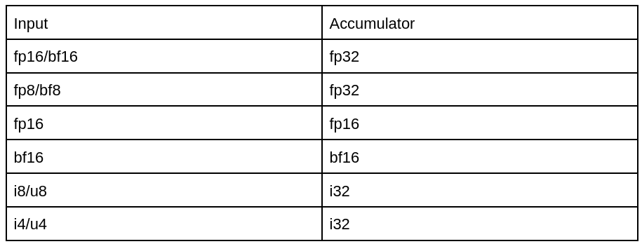
The "headline" feature of the MI455X is undoubtedly its AI performance, powered by enhanced tensor units. AMD has moved away from the older "MFMA" (Matrix-Fused Multiply-Accumulate) instructions found in CDNA4, opting for "WMMA" (Wave Matrix Multiply-Accumulate) support, similar to RDNA4.
The WMMA Matrix
The GFX1250 retains the 16×16 matrix (M=N=16) dimensions from RDNA4 but maintains the higher-performance K-values associated with CDNA4.
- FP64/FP32: K=4
- FP16: K=32
- Int8: K=64
- FP8: K=128
By supporting OCP MX-style scaling—a format previously restricted to the CDNA4 architecture—the GFX1250 demonstrates AMD’s commitment to providing a flexible, industry-standard path for AI developers.
Memory Hierarchy and Atomic Operations
The Local Data Share (LDS) capacity has been doubled to 320kB per wavefront. However, the most significant change is the integration of the LDS and the vector L0 cache into a single, cohesive 448KB structure known as the WGP Cache (WGP$). This moves AMD closer to the unified memory structures seen in NVIDIA’s architectures, allowing for dynamic allocation based on compiler needs.
Furthermore, the introduction of 128B atomic loads and stores provides a robust mechanism for inter-wavefront communication. These operations, while not inherently "special" at the hardware instruction level, are orchestrated to ensure data integrity across the memory bus—a vital requirement for scaling large AI models across thousands of GPUs.
Implications for the Market and Development
The transition to the GFX1250 has several far-reaching implications for the AI ecosystem.
Challenging the Dominance of Blackwell
AMD’s introduction of "Thread Block Clusters"—an architectural feature similar to NVIDIA’s Hopper and Blackwell clusters—suggests that AMD is focused on solving the communication bottlenecks inherent in massive, multi-node training. By allowing wavefronts to access LDS memory from other workgroups within a cluster, AMD is effectively creating a "Distributed Shared Memory" environment. This, combined with the new cluster-level barriers and arrival monitors, indicates that AMD is building the necessary software infrastructure to compete directly with NVIDIA’s proprietary NCCL (NVIDIA Collective Communications Library).
The "Pure Compute" Shift
By removing legacy graphics hardware and focusing on pure compute, AMD is optimizing the GFX1250 for efficiency. The inclusion of hardware-level tanh activation support and improved FP32 latency (dropping from 9 cycles in RDNA4 to 8 cycles in GFX1250) underscores a relentless pursuit of performance in areas where AI models spend the most time.
The Developer Experience
For developers, the GFX1250 presents a double-edged sword. While the new architecture offers significantly more power and flexibility, it also mandates a shift in how kernels are written. The move to Wave32-only and the introduction of fine-grained wait counts for memory synchronization mean that codebases optimized for older GCN or CDNA chips will likely need significant refactoring. However, the benefits—such as the ability to issue texture or memory reads without stalling the core—are substantial.
Official Responses and Future Outlook
While AMD has remained tight-lipped regarding specific performance benchmarks until the "Advancing AI" event, the depth of the LLVM commits suggests that the software stack (ROCm) is already well-prepared for the hardware’s arrival. The company has focused on ensuring that the MI455X is not just a collection of fast transistors, but a programmable, cohesive system that fits into the existing OCP (Open Compute Project) ecosystems.
As we look toward the future, the GFX1250 seems to be the blueprint for a new era of AMD GPUs. Whether the high-register-count capabilities and cluster-based communication will filter down to the consumer Radeon lineup remains a point of speculation, but the hardware foundations are clearly being laid.
In conclusion, the GFX1250 is a calculated, aggressive response to the current AI landscape. By combining the best aspects of their RDNA and CDNA lineages and adopting sophisticated cluster-level synchronization, AMD is positioning the MI455X to be more than just a theoretical alternative to NVIDIA—it is a functional, highly capable engine designed to power the next generation of generative AI and scientific discovery. The "tea leaves" of the LLVM commits point to a bright, albeit complex, future for AMD in the data center.
 rifanmuazin
  Layla Zulfa
  Evan Lee Salim