
 By Basiran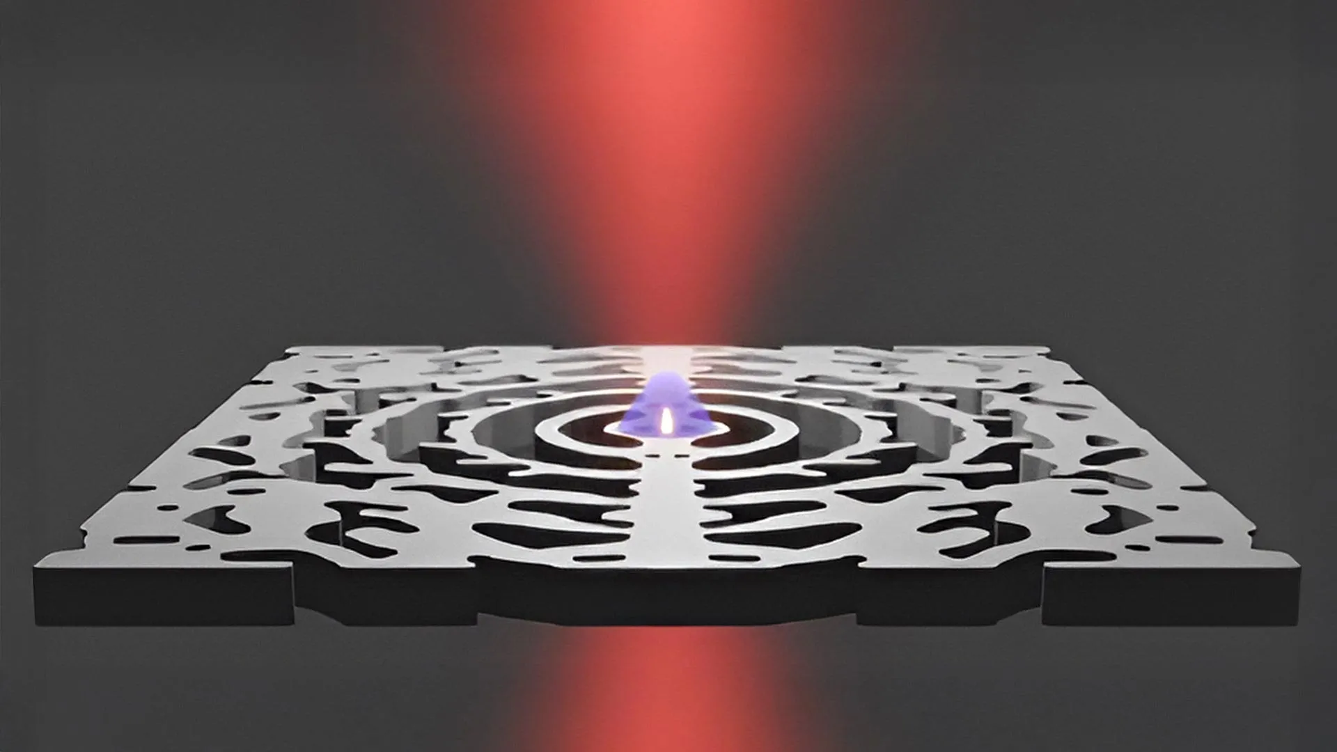
In a development that could fundamentally rewrite the architecture of modern computing, researchers at the Technical University of Denmark (DTU) have unveiled a breakthrough in nanotechnology: a ultra-compact nanolaser capable of operating at room temperature. This innovation, recently published in the prestigious journal Science Advances, represents a critical milestone in the transition from traditional electronic-based microchips to high-speed, light-based photonic communication. By harnessing the properties of photons to transmit data, this technology promises to drastically accelerate the performance of smartphones, supercomputers, and global data centers while simultaneously slashing their power consumption.
Main Facts: A New Frontier in Nanophotonics
The core of the DTU discovery lies in the successful creation of a laser so small that thousands could be integrated onto a single silicon microchip. Traditionally, lasers have been bulky components, often restricted to large-scale telecommunications infrastructure. The DTU team, led by Professor Jesper Mørk alongside Drs. Meng Xiong and Yi Yu from DTU Electro, has managed to push past the conventional physical limits of laser miniaturization.
The device functions through a specialized "nanocavity"—a structure designed to trap and concentrate light within an exceptionally small volume. When external light is introduced, photons and electrons are confined to the same microscopic region, allowing the laser to reach the "lasing threshold" with minimal energy input. Unlike previous iterations of nanolasers that required cryogenic cooling, this new device maintains stability at room temperature, a vital prerequisite for commercial viability in consumer electronics.
Chronology of Innovation
The journey to this breakthrough did not happen in a vacuum; it is the culmination of years of interdisciplinary collaboration at DTU.
The Foundational Years
The conceptual framework for this technology began with the theoretical exploration of light-matter interaction at the nanoscale. For decades, the primary challenge in optics was the "diffraction limit," which suggested that light could not be focused smaller than half its wavelength. Overcoming this barrier required a radical rethinking of structural design.
The Design Breakthrough
A pivotal moment occurred when the team incorporated light-trapping structures originally developed by Professor Ole Sigmund’s group at DTU Construct. Utilizing advanced computational topology optimization, the researchers were able to create a cavity design that was mathematically engineered to confine light more efficiently than any natural or previously man-made structure.
The Fabrication Phase
In the DTU Nanolab—the university’s state-of-the-art clean room facility—the researchers moved from simulation to fabrication. Using high-precision lithography, they etched the nanocavities into semiconductor materials. This process required sub-nanometer precision, ensuring that the structural integrity of the cavity would support the intense electromagnetic fields necessary for laser operation.
Current Validation
Following the successful fabrication, the team subjected the device to rigorous testing. By measuring the light output against input energy, they confirmed that the laser reached the required threshold for sustained operation without the need for external cooling. The successful publication in Science Advances serves as the scientific community’s validation of these results, marking the transition of the project from experimental physics to engineering development.
Supporting Data: Why Light Outperforms Electrons
To understand the significance of the DTU nanolaser, one must first examine the limitations of current hardware. Modern microchips are essentially vast networks of microscopic wires moving electrons. While this has powered the digital age, it has reached a physical bottleneck.
The Heat Problem
Electrons moving through copper or silicon wiring encounter resistance, which generates heat. As chips become smaller and denser, the ability to dissipate this heat becomes a limiting factor for performance. This is why high-end processors often "throttle" their speed when they get too hot. Photons, however, do not generate the same thermal footprint. By replacing electrons with light signals, data can be transmitted with almost zero heat generation.
Energy Efficiency
Professor Mørk estimates that integrating these nanolasers into computer architecture could reduce energy consumption by up to 50 percent. In an era where data centers account for a significant and growing portion of global electricity usage, such a reduction is not merely a technological convenience—it is a climate imperative.
Bandwidth and Speed
Electrical signals are limited by RC (resistance-capacitance) delays. Photons travel at the speed of light and can carry significantly more information through multiplexing (sending multiple signals on different wavelengths simultaneously). The DTU nanolaser provides the "on-chip" light source necessary to unlock this massive increase in bandwidth, potentially enabling a thousand-fold increase in data transfer rates within the architecture of a computer.
Official Responses: Insights from the Research Team
Professor Jesper Mørk, a leading voice in the study, highlights the versatility of the team’s discovery. "The nanolaser opens up the possibility of creating a new generation of components that combine high performance with minimal size," Mørk notes. He emphasizes that the impact will extend far beyond the computing industry.
"In the healthcare sector," Mørk explains, "the nanolaser’s extreme light concentration can deliver high-resolution images and ultrasensitive biosensors." Because the laser can detect minute changes in its environment, it could potentially be used to identify pathogens or biomarkers in blood samples at a level of sensitivity that is currently unattainable with standard diagnostic tools.
Drs. Meng Xiong and Yi Yu, who co-authored the paper, have focused heavily on the engineering hurdles of scaling the technology. They emphasize that while the physics are now proven, the challenge ahead lies in "system integration." This involves not just the laser itself, but the optical waveguides, modulators, and detectors that must be integrated alongside the laser to form a complete photonic circuit.
Implications: A Future Built on Light
The roadmap for the next 5 to 10 years is clear, though challenging. The immediate next step for the DTU team is to transition the nanolaser from an optically pumped device—which requires an external light source—to an electrically pumped device.
The Electrically Driven Challenge
Integrating electrical contact points onto a device that is essentially the size of a few hundred atoms is an engineering feat of the highest order. The team must ensure that the electrical connections do not interfere with the optical nanocavity’s ability to trap light. Solving this will be the "holy grail" of the research, as it will allow the laser to be powered directly by the same batteries or power supplies that run our current computers.
Transformation of Data Centers
The current structure of the internet relies on light for long-distance transport through fiber-optic cables, but the signal must be converted back to electricity at every "hop" or interface within a server. This conversion process is energy-intensive and slow. By embedding nanolasers directly into the chips that process data, these conversions could be eliminated entirely, creating an "all-optical" data path from the server rack to the processor.
Revolutionizing Consumer Electronics
For the average consumer, this means smartphones that are significantly faster, have longer battery lives, and can handle complex AI tasks locally rather than in the cloud. As we move toward a future defined by edge computing and real-time AI processing, the energy efficiency provided by nanolasers will be the difference between stagnant technology and the next generation of digital tools.
Medical Diagnostics
Beyond IT, the implications for medicine are profound. Imagine a wearable device or a smartphone attachment capable of real-time, ultra-accurate diagnostic testing. The high-resolution imaging capabilities made possible by these nanolasers could allow doctors to visualize cellular structures in real-time without the need for bulky, expensive laboratory equipment.
Conclusion: The Horizon of Photonics
The DTU breakthrough is a reminder that the most significant leaps in technology are often those that occur at the smallest scales. By successfully confining light in a way that was previously deemed impossible, the researchers at DTU have provided the missing link for the next era of computing.
While the "5-10 year" timeline for solving the remaining electrical integration challenges may seem distant to some, in the world of semiconductor development, it is a rapid trajectory. The work of Mørk, Xiong, Yu, and their colleagues suggests that the "electronic age" is entering its final chapter, and the "photonic age" is waiting in the wings. As we stand on the precipice of this transition, it is clear that the future of technology will not just be faster or more efficient—it will be powered by the very particles of light themselves.
 Sagoh
Sagoh  Asro
Asro  Siti Muinah