
 By Reynand Wu
The landscape of modern computing is approaching a fundamental physical barrier. For decades, the industry has relied on the relentless miniaturization of electrical transistors—a trend famously dubbed Moore’s Law. However, as chips become smaller and denser, the movement of electrons through copper wires is generating excessive heat and creating bottlenecks that limit data processing speeds.
Now, a team of researchers at the Technical University of Denmark (DTU) has unveiled a groundbreaking development that could shift the paradigm from electronics to photonics. By creating an ultra-compact nanolaser capable of operating at room temperature, the team has taken a definitive step toward a future where microchips communicate not through electricity, but through particles of light. Published in the journal Science Advances, this innovation promises to redefine the limits of energy efficiency and computational speed.
The Evolution of Communication: From Fiber Optics to Microchips
To understand the magnitude of this breakthrough, one must look at the current architecture of global data transmission. For years, the internet backbone has relied on fiber optic cables, which utilize light to carry vast amounts of information across continents with minimal loss. This "optical advantage" is well understood: light travels faster than electrons in a wire, generates no heat through resistance, and allows for massive bandwidth.
Yet, once this light reaches the doorstep of a data center or the interior of a smartphone, it must be converted back into electrical signals. This conversion process is not only energy-intensive but also serves as the primary source of thermal throttling in modern devices.
Inside a standard microchip, moving information via electrical signals creates resistance, which inevitably manifests as heat. This heat requires cooling systems, limits the density of transistors, and consumes a significant portion of the total energy budget. The vision of "on-chip photonics"—where light is generated and manipulated directly on the silicon substrate—has long been the "holy grail" of computer engineering. The DTU nanolaser provides the mechanism to make this vision a reality.
Chronology: A Multi-Disciplinary Sprint to the Nanoscale
The path to this discovery was not linear; it required the convergence of expertise across several disciplines at DTU.
Phase I: Theoretical Foundations and Light Trapping
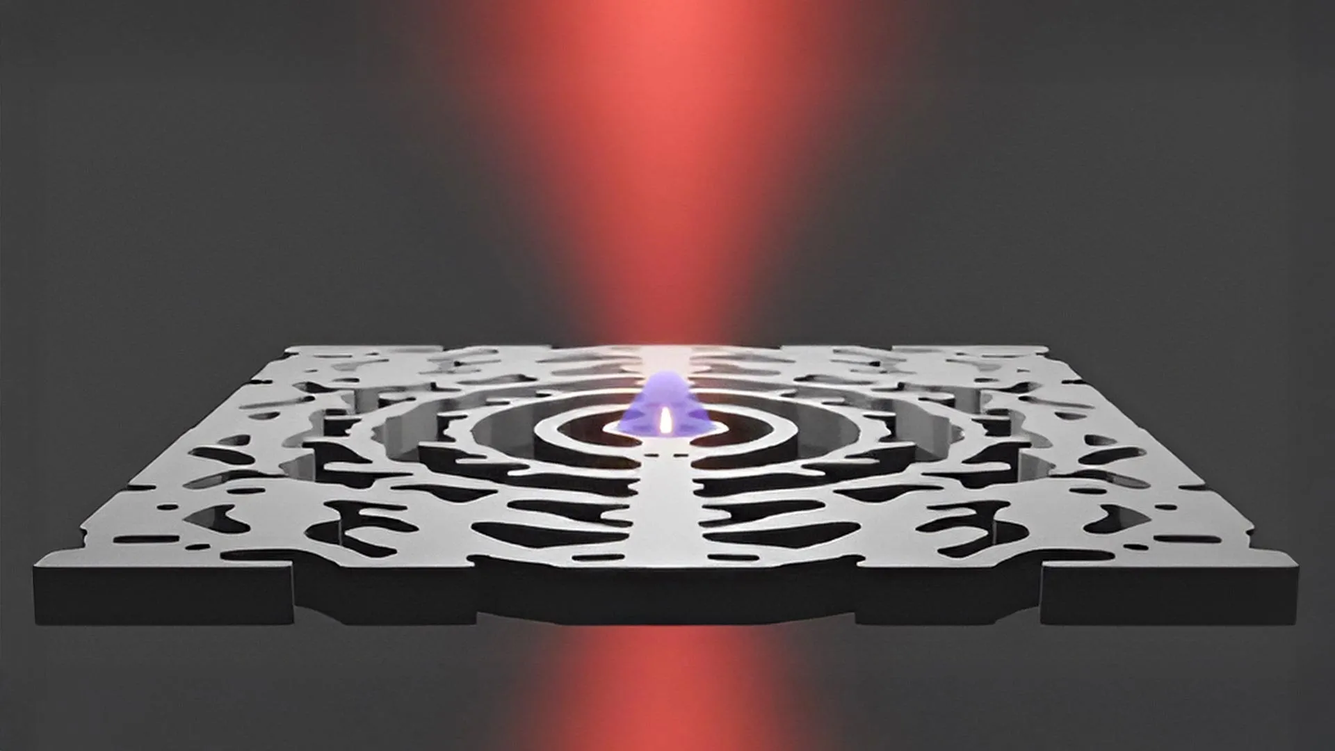
The project’s origins trace back to the collaborative efforts between the Department of Electrical Engineering (DTU Electro) and the Department of Civil and Mechanical Engineering (DTU Construct). A critical piece of the puzzle was the light-trapping structure, originally developed by Professor Ole Sigmund’s group. Their work in topology optimization allowed for the creation of a "nanocavity"—an architectural design that traps and concentrates light in a space significantly smaller than the wavelength of the light itself.
Phase II: Fabrication at DTU Nanolab
With the theoretical framework in place, the team moved to the DTU Nanolab clean room facility. Here, Drs. Meng Xiong and Yi Yu, alongside Professor Jesper Mørk, worked to manufacture the physical device. The challenge was twofold: creating a structure small enough to be integrated into existing semiconductor processes, while ensuring the device could function without the need for cryogenic cooling.
Phase III: Successful Verification
The culmination of this work resulted in a device that successfully concentrates both photons and electrons within a microscopic region. When stimulated by an external light beam, the device reaches the threshold required for lasing—the emission of coherent, concentrated light. The successful demonstration of this process at room temperature was the "eureka" moment that signaled the technology was ready for scientific publication and further development.
Supporting Data: Why Size Matters
In the world of lasers, size has historically been an obstacle to efficiency. Large-scale lasers are efficient for industrial cutting or long-range telecommunications, but they are incompatible with the microscopic world of a central processing unit (CPU).
The DTU nanolaser breaks the conventional size limit for light-emitting devices. By utilizing a nanocavity to achieve extreme light confinement, the laser requires an exceptionally low amount of energy to activate. According to Professor Jesper Mørk, the transition to such a system could be transformative for energy conservation:
- Energy Efficiency: Mørk estimates that the integration of these nanolasers into computers could reduce total energy consumption by as much as 50 percent.
- Thermal Management: Because photons do not generate resistance-based heat, the shift to optical signaling could eliminate the need for the bulky, energy-draining cooling solutions currently required in high-performance computing.
- Density Potential: Current silicon photonics are limited by the size of the laser sources. By shrinking these sources to the nanoscale, thousands of lasers could potentially be integrated onto a single chip, creating a massively parallelized data network that operates at the speed of light.
Official Perspectives: The Road Ahead
The researchers involved in the project emphasize that while this is a massive technical victory, it is not yet a commercial product. The transition from a laboratory experiment to a mass-produced component involves solving the "electrical injection" challenge.
"The nanolaser opens up the possibility of creating a new generation of components that combine high performance with minimal size," says Professor Jesper Mørk. "This could be in information technology, where ultra-small and energy-efficient lasers can reduce energy consumption in computers, or in the development of sensors for the healthcare sector, where the nanolaser’s extreme light concentration can deliver high-resolution images and ultrasensitive biosensors."
Dr. Meng Xiong and Dr. Yi Yu, who co-authored the study, view this as a foundational step. The current iteration of the nanolaser is stimulated by light, but the next phase of development focuses on achieving the same results using electrical power. This is the critical transition required for compatibility with existing CMOS (Complementary Metal-Oxide-Semiconductor) fabrication techniques used by companies like Intel and TSMC.
Implications: A New Era of Technology
The implications of this technology extend far beyond faster smartphones. If the team succeeds in integrating these lasers into existing chip architectures, the impact will be felt across several global industries.
1. The Green Revolution in Data Centers
Data centers are among the world’s largest consumers of electricity, driven largely by the need to move data and keep servers cool. A 50% reduction in energy consumption is not merely an incremental improvement; it is a fundamental shift in the sustainability profile of the internet. As AI and machine learning models demand ever-increasing computational power, optical computing may be the only way to scale these technologies without hitting a "power wall."
2. Next-Generation Healthcare Diagnostics
The extreme concentration of light enabled by the nanocavity has immediate applications in biosensing. High-resolution imaging systems, which currently rely on bulky lenses and external light sources, could be miniaturized into "lab-on-a-chip" devices. These could perform real-time, ultrasensitive analysis of biological samples, detecting diseases at the molecular level with unprecedented speed and accuracy.
3. The Future of Consumer Electronics
For the average consumer, this technology represents a future where battery life could be extended significantly. When the communication between a processor, memory, and storage is optical rather than electrical, the efficiency gains will be felt in every device that requires high-speed data processing—from the latest smartphone to autonomous vehicles, which must process massive amounts of sensor data in real-time.
The Five-to-Ten-Year Horizon
The research team at DTU is optimistic about the timeline. While the transition from lab to industry is notoriously difficult, the researchers estimate that the remaining technical hurdles—specifically electrical injection and large-scale manufacturing integration—could be solved within the next 5 to 10 years.
This timeframe aligns with the broader industry roadmap for optical interconnects. As current copper-based interconnects reach their physical limits, the "photonics revolution" is no longer a question of if, but when. The DTU nanolaser provides the specific "engine" required to make that shift possible.
By pushing the boundaries of light-matter interaction, the DTU team has provided more than just a new laser; they have provided a blueprint for the next century of computing. As we look toward a future where our devices are faster, cooler, and fundamentally more efficient, it is clear that the solution lies in the smallest of spaces, illuminated by the power of light.
 Ammar Sabilarrohman
 rifanmuazin
 Iffa Jayyana
