
 By Evan Lee Salim
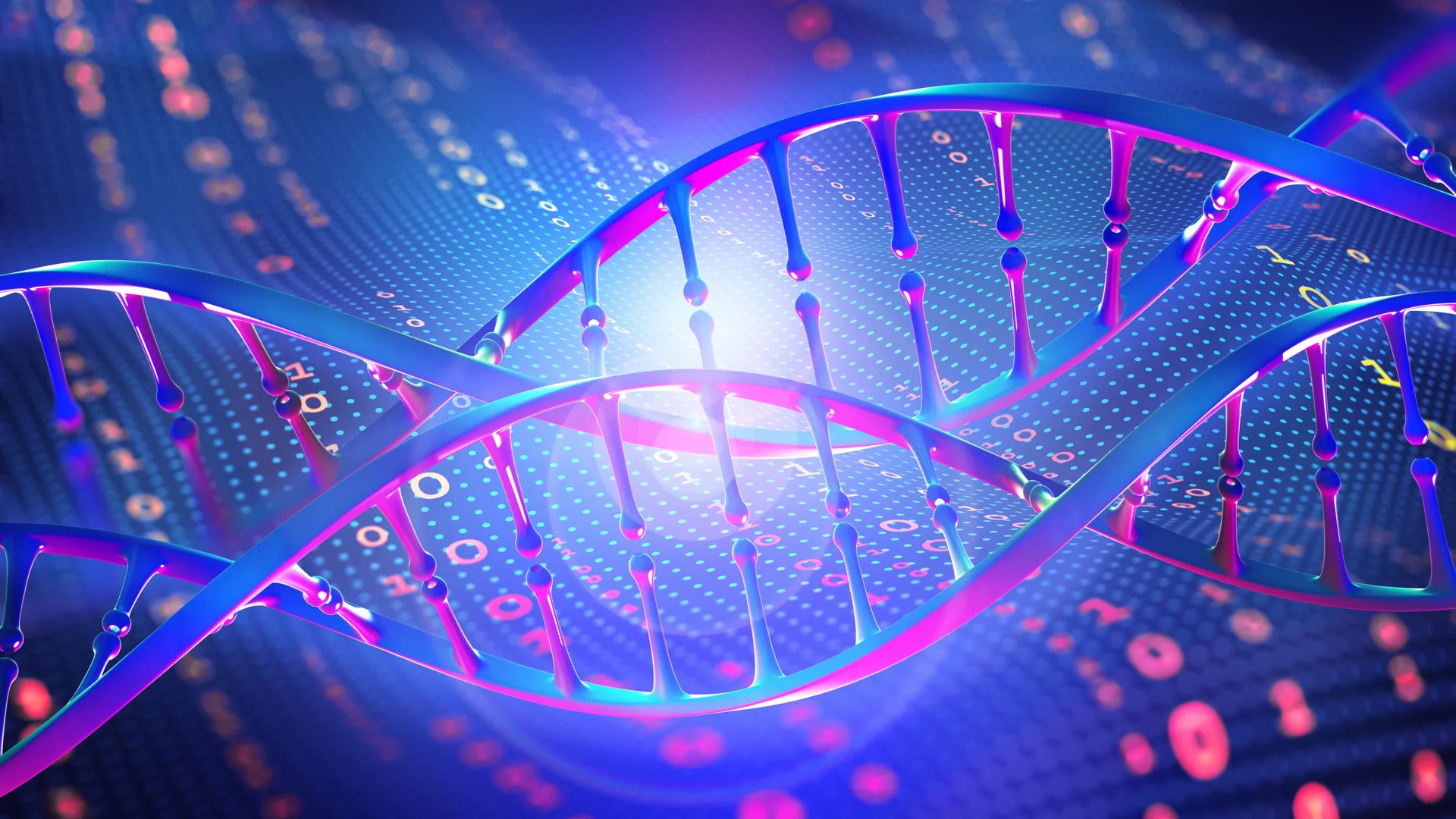
In the race to build the next generation of artificial intelligence, the physical limitations of silicon are becoming increasingly apparent. As our digital hunger for data grows, so too does the energy footprint of the massive server farms that power the internet. Now, a groundbreaking development from Penn State University promises a radical shift in how we think about storage and processing: the integration of synthetic DNA into electronic semiconductors.
By bridging the divide between biological macromolecules and inorganic materials, researchers have successfully engineered a bio-hybrid "memristor"—a memory resistor capable of storing and processing information with unprecedented energy efficiency. This marriage of life’s genetic blueprint and advanced crystalline semiconductors offers a glimpse into a future where computers operate more like the human brain, consuming a fraction of the power required by today’s technology.
The Convergence of Biology and Silicon
DNA is nature’s most efficient information storage medium. A single gram of the double-helix molecule can store approximately 215 million gigabytes of data, packing the sum of human history into a footprint the size of a grain of sand. However, the fundamental challenge has always been compatibility: biological materials are soft, fluid, and fragile, while electronic components are rigid, metallic, and require extreme environments to function.
The research team, led by a multidisciplinary group at Penn State, has shattered this barrier. By utilizing synthetic DNA sequences and crystalline perovskite—a high-performance semiconductor already utilized in solar panels and advanced lasers—they have created a stable, conductive platform that functions at the nanoscale. The findings, recently published in Advanced Functional Materials, mark a departure from traditional binary computing, pointing toward a future of neuromorphic, bio-inspired electronics.
A Chronology of Innovation
The journey toward this bio-hybrid breakthrough began with a fundamental question: Could the high-density storage capacity of DNA be harnessed to solve the "memory wall" in modern computing?
- Initial Conceptualization: The researchers identified the inherent incompatibility between biological molecules and semiconductor electronics as the primary hurdle. Natural DNA, characterized by long, tangled, and unstable strands, was deemed unsuitable for the precision required in circuit manufacturing.
- Engineering the Solution: The team turned to synthetic, molecularly engineered DNA. By customizing the length and composition of these sequences, they created rigid, controllable "building blocks" that could be systematically arranged.
- The Integration Phase: The researchers experimented with "doping"—a technique used to enhance semiconductors—by introducing silver nanoparticles into the DNA-perovskite matrix. This critical step served a dual purpose: it granted the DNA electrical conductivity and forced its molecular units into a highly organized, predictable structure.
- Device Fabrication: Once the material platform was established, the team constructed a memristor. Unlike standard resistors that lose data when power is cut, this device "remembers" the electrical path taken through it, mimicking the synaptic behavior of neurons.
- Validation and Testing: The resulting device underwent rigorous testing, demonstrating stability at extreme temperatures and operational efficiency far beyond current silicon-based storage standards.
The Science of the Bio-Hybrid Memristor
At the heart of this innovation is the memristor. In a conventional computer, data must travel between the processor and the memory drive, creating a bottleneck that consumes significant energy and time. Memristors solve this by performing storage and processing in the same physical location, mirroring the way neurons function in the human brain.
Engineering DNA for Conductivity
The secret to the device’s performance lies in the "doping" process. Natural DNA is not an ideal conductor. By doping the synthetic DNA with silver nanoparticles, the researchers created a "molecular bridge." These nanoparticles allow the DNA to conduct electrons reliably while also acting as a structural scaffold that keeps the device stable.
According to Neela H. Yennawar, director of the Penn State Huck Institutes’ Biomolecular Interactions Core Facility, the ability to computationally determine the exact sequence of DNA needed is a game-changer. "We can rationally design these structures to interface seamlessly with perovskites," Yennawar noted. "This transforms DNA from a passive biological molecule into a programmable, multifunctional nanomaterial."
Efficiency and Stability
The performance metrics of the device are striking. The team found that the system operates reliably at under 0.1 volts—a negligible amount compared to the 120 volts found in standard wall outlets. Furthermore, the hybrid device demonstrated remarkable thermal stability, remaining functional at temperatures up to 250 degrees Fahrenheit. It also maintained its structural and functional integrity at room temperature for over six weeks, significantly outperforming existing perovskite-only storage devices.
Official Perspectives: Bridging Two Worlds
The collaborative nature of the study brought together experts in materials science, biology, and chemical engineering. The co-authors emphasize that this is not merely an improvement on existing technology, but a fundamental paradigm shift.
"Biology and electronics are different domains," said Kavya S. Keremane, a postdoctoral researcher in materials science and engineering. "Bridging these two fields required developing an entirely new materials platform that allows them to function seamlessly together. By combining the information storage capabilities of DNA with the exceptional electronic properties of perovskite, we created a bio-hybrid system that fundamentally changes how low-power memory devices can be designed."
Bed Poudel, a research professor of materials science and engineering, highlighted the necessity of this work in the context of the global AI boom. "As the demand for artificial intelligence grows, we need a new strategy for low-power, high-storage devices," Poudel explained. "Usually, it takes more power to store more information. Our device, however, consumes 100 times less power and the storage capacity is higher than traditional storage devices."
Implications for the Future of Computing
The successful integration of DNA into electronic circuits has profound implications for the future of technology, particularly in three key areas:
1. Neuromorphic Computing
As we push toward systems that mimic the human brain, the need for components that can evaluate multiple inputs simultaneously becomes critical. The memristor’s ability to "learn" from previous electrical activity allows for a more fluid, adaptive form of computing. This will be essential for AI systems that need to make real-time decisions based on complex, evolving datasets.
2. Radical Energy Efficiency
Modern data centers are among the world’s largest consumers of electricity. If memory components can be built that consume one-tenth the power of current technologies, the cumulative savings—both in electricity and heat management—would be transformative. This is especially vital for mobile devices, space exploration hardware, and remote sensing technology, where battery life and power management are constant constraints.
3. High-Density Archiving
While the current focus is on memory for processing, the underlying potential for long-term data storage is equally significant. With DNA’s ability to hold immense amounts of data in a tiny volume, we may one day see "bio-hard drives" that store the entirety of an organization’s digital archive on a chip the size of a thumbnail, without the need for constant cooling or high-power maintenance.
A New Horizon for Bio-Inspired Electronics
The Penn State team, which included researchers from the University of Minnesota, has already set its sights on the next phase of the project. Their current success is considered a proof-of-concept—a glimpse into a broader potential for bio-inspired electronics.
"Nature has the solution—we just have to find it and apply it," Poudel stated. The team plans to refine the material synthesis process to allow for mass-manufacturability and to explore how these DNA-perovskite hybrids can be scaled into larger, more complex computing architectures.
The research was supported by the U.S. National Science Foundation, the National Institutes of Health, and the respective universities involved. As the project moves from the laboratory to potential commercial applications, the intersection of biology and electronics stands as one of the most promising frontiers in modern science. By looking to the double helix for inspiration, scientists have not only created a more efficient memory device but have also fundamentally expanded the definition of what constitutes an "electronic" material.
In a world increasingly dominated by the massive processing requirements of AI, this fusion of DNA and perovskite represents a small but powerful step toward a future where computing is as efficient and elegant as the life it seeks to emulate.
 Reynand Wu
 Ammar Sabilarrohman
 rifanmuazin
